


Please Leave Us A Message
Privacy statement: Your privacy is very important to Us. Our company promises not to disclose your personal information to any external company with out your explicit permission.

Guangzhou Ruihong Electronic Technology CO.,Ltd
 June 15, 2022
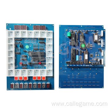
Double-layer pcb means to draw wires on the top and bottom of a pcb board. The double panel solves the difficulty of wiring interleaving in a single panel (it can be conducted to the other side through the hole), that is, the wiring is provided on both the front and the back, the components can be soldered on the front side, or the reverse side, the double-layer circuit board There are components and wiring on both sides of the board. It is unquestionable that it is more difficult to design a double-layer PCB board. Let's analyze the wiring rules of the double-layer pcb board and share with you how to draw a double-layer pcb board.
How to draw a double-layer pcb board For double-layer pcb boards, the wires on both sides must be used. It is necessary to have proper circuit connections between the two sides. The "bridge" between such circuits is called a via. The via hole is a small hole filled or coated with metal on the pcb, which can be connected to the wires on both sides. When using PROTEL to draw a double-sided pcb board, draw a wire connection component on the TopLayer (top layer), which is the top layer drawing board; select BottomLayer (bottom layer), draw the wire connection component on the bottom layer, and draw the board on the bottom layer. The above is the basis for drawing a double layer pcb.
Before drawing a double-layer pcb board, first determine the layout of the components, and firstly distribute the key crystal, crystal oscillator circuit, clock circuit, CPU and other signal lines when wiring. Be sure to follow the principle that the circulation area is as small as possible.
After the two-layer board is determined by the reasonable layout of the components, the power line of the ground-screen copy board is designed first, and then the important lines---sensitive lines, high-frequency lines, and general lines---low-frequency lines. The key leads preferably have separate power supplies, ground loops, and very short leads, so sometimes a ground wire is placed on the critical line next to the signal line to allow it to form a minimum working loop.
When drawing a double-layer PCB board, follow the layout principle of “first big, then small, first difficult and easy”, that is, important unit circuits and core components should be prioritized. The layout should refer to the principle block diagram, according to the main board. The main components of the signal flow are regularly arranged.
The total connection is as short as possible, and the key signal line is the shortest; the high voltage and high current signals are completely separated from the low current and low voltage weak signals; the analog signal is separated from the digital signal; the high frequency signal is separated from the low frequency signal; and the high frequency component is separated. Be full.
It should be noted that the two double-layer boards have a ground plane on the lower layer of the board. This is designed so that engineers can quickly see the wiring when troubleshooting, which is often seen on the device manufacturer's demonstration and evaluation board. But a more typical approach is to lay a ground plane on the upper layer of the board to reduce the electromagnetic dry (emi).
The above is the How to draw double-layer pcb board we have listed for you. You can submit the following form to obtain more industry information we provide for you.
You can visit our website or contact us, and we will provide the latest consultation and solutions
Send Inquiry
Most Popular
lastest New
Related Products
Send Inquiry
Privacy statement: Your privacy is very important to Us. Our company promises not to disclose your personal information to any external company with out your explicit permission.
Fill in more information so that we can get in touch with you faster
Privacy statement: Your privacy is very important to Us. Our company promises not to disclose your personal information to any external company with out your explicit permission.